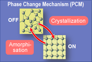
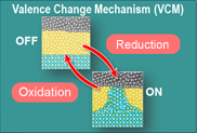
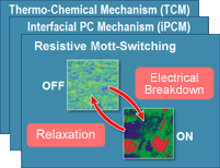
Traditional semiconductor-based electronics is based on electronic effects, while atomic configuration changes are detrimental to the desired device performance. The success of electronics in the past forty years has been based on a continuous decrease of the feature size (“Moore’s law”) and an accompanying reduction in energy consumption. However, this concept is approaching its physical limits. In striking contrast to this philosophy, a set of resistive switching phenomena exists in oxides and higher chalcogenides in which the change of atomic configurations including atomic and ionic defects represents the essential functionality. It is the goal of SFB 917 to understand and explore the potential of advanced nanoswitches based on such configuration changes.
Traditional semiconductor-based electronics is based on electronic effects, while atomic configuration changes are detrimental to the desired device performance. The success of electronics in the past forty years has been based on a continuous decrease of the feature size (“Moore’s law”) and an accompanying reduction in energy consumption. However, this concept is approaching its physical limits. In striking contrast to this philosophy, a set of resistive switching phenomena exists in oxides and higher chalcogenides in which the change of atomic configurations including atomic and ionic defects represents the essential functionality. It is the goal of SFB 917 to understand and explore the potential of advanced nanoswitches based on such configuration changes.
Since SFB 917 was established on July 1, 2011, this field has witnessed rapid growth and spectacular findings, with strong contributions coming from the 19 projects involved in the SFB. These advances can be divided into three categories; a dramatically improved understanding of materials, the increased significance of data for modern societies, and the desire to develop concepts that go beyond the classical von Neumann architecture.
The overarching aim of SFB 917 is to advance the microscopic understanding of resistive switching phenomena utilising changes in the atomic configurations, in particular in the phase and the valence of oxides and higher chalcogenides. To explore the full potential and pave the way for such an electronics technology it is mandatory to realise ultrahigh scalability, fast switching kinetics and long retention times. These are the most important goals to tap into the technological potential of this unconventional class of materials. Yet, as we have learnt in the last few years, the goals that have to be reached go considerably beyond. The energy consumption linked to information technology has increased significantly in recent years. To revert this ongoing trend, completely new devices as well as architectures have to be developed. The promise to realise fast, non-volatile memories as well as energy-efficient devices, which may ultimately enable novel, brain-like functionalities by neuromorphic computing, defines the technological potential of the present SFB.
The phenomena utilised in these emerging devices show the characteristic features of complex electronic materials where ionic, electronic, and vibronic degrees of freedom are closely interwoven. Yet the desired functionalities can only be realised if the materials contain the appropriate type and density of atomic and ionic defects. Before the unique opportunities of configuration-based electronics can be capitalised on, several challenges must be overcome. The impact of defects on material properties, the atomistic mechanisms of the corresponding switching phenomena and their kinetics, as well as device schemes that control the defect concentrations on the nanometre scale have to be unraveled. Successful activity will pave the road to novel memories and alternative computer architectures.
 Structure and material complexity (A)